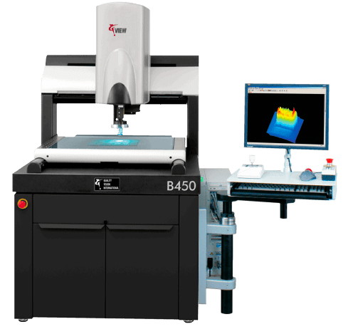
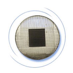
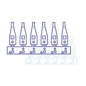
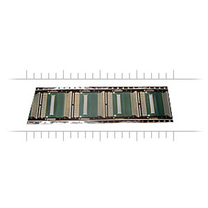
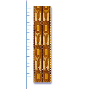
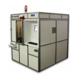
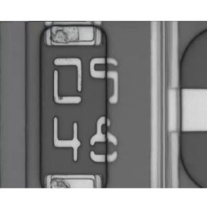
No matter what the requirement for ultra high-precision measurement, VIEW has the ideal solution. VIEW non-contact measurement systems utilize sub-pixel image feature detection with either field-of-view (FOV) or point-to-point (PTP) configurations for exceptional accuracy and repeatability. From etch-dimensions on hard disk drive (HDD) heads to semiconductor overlay measurements, we provide the accuracy you need for quality manufacturing.
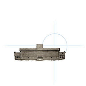
Connector Measurement
Quickly acquire data on connector positions, size, pitch, & coplanarity measurements
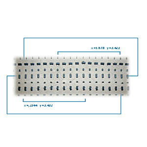
Electronic Assembly Calibration & Monitoring
Measurement of positioning and rotation (X, Y, and Theta) relative to pads
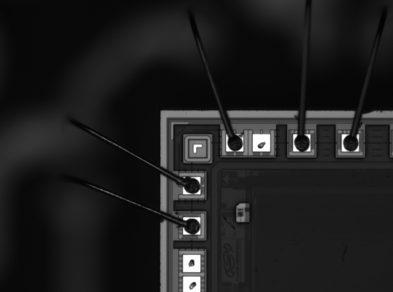
Measuring ball, tooling mark diameters, placement, pad alignment, & wire loop height
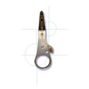
Hard Disc Drive Component Metrology
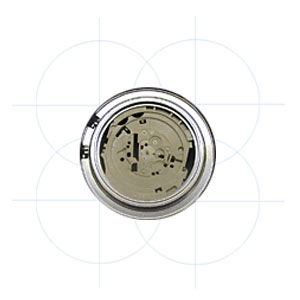
Mobile Phone, Tablet & Wearable Assembly
Accurate and efficient non-contact inspection of fan-out wafer-level packaging with multiple levels of magnification
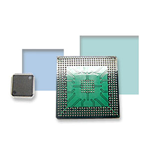
Coplanarity, lead width, pitch, ball diameter, package height and warpage inspection
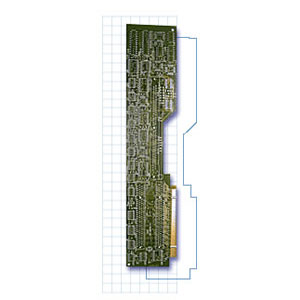
PCB Inspection
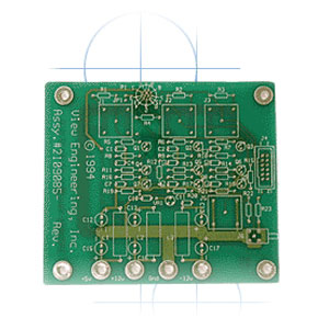
Measurement of critical features such as the positions of leads, pads, and warpage
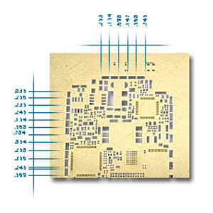
Flexibility to rapidly measure a wide variety of aperture sizes, shapes, and positions
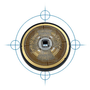
Photolithography & MEMs Fabrication
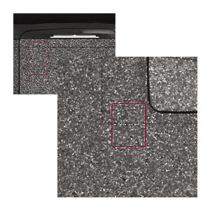
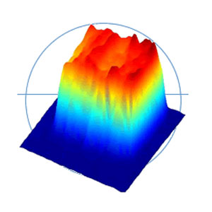
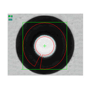
VIEW system analyzes the pixels within the measurement window and builds a radial intensity profile of the circle
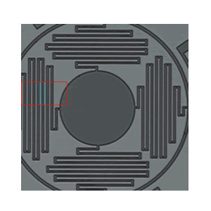
Measurement of pitch, width, and spacing of flexures, fingers, combs, arcs, circle diameters, and center locations
Flexibility to rapidly measure a wide variety of aperture sizes, shapes, and positions
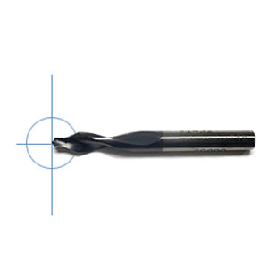
Precision Micro-Grinding
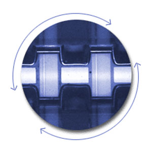
Metrology system high-resolution stage motion, quality optics, autofocus capabilities
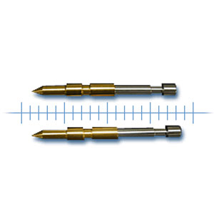
Inspection of electrical test probes requires precision metrology capabilities to accurately measure small features
Custom Engineering
Application-specific fixturing, programming, interfaces to third party sensors & equipment
