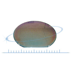
Bump on die inspection presents some of the most demanding non-contact metrology challenges in today’s semiconductor manufacturing environments. The requirement to inspect very small part features while maintaining extremely tight tolerances is difficult under the best of circumstances.
However, the need to maintain high throughput to rapidly inspect samples from large volume production can make it even more challenging. With ball diameters as small as 3mil to 12mil, accurately inspecting critical factors such as bump height, location, and coplanarity often requires advanced metrology features, such as very high-resolution stage motion, dual magnification optics, and through-the-lens laser probe options.
In order for you to view this file we ask that provide us with some information.
[dlm_gf_form download_id="2111" gf_ajax="true"]
Thank you for your interest in
Bump on Die
In order for you to view this file we ask that provide us with some information.
[dlm_gf_form download_id="2115" gf_ajax="true"]
Thank you for your interest in
Bump on Die
In order for you to view this file we ask that provide us with some information.
[dlm_gf_form download_id="2114" gf_ajax="true"]
Thank you for your interest in
Bump on Die
In order for you to view this file we ask that provide us with some information.
[dlm_gf_form download_id="2113" gf_ajax="true"]
Thank you for your interest in
Bump on Die
In order for you to view this file we ask that provide us with some information.
[dlm_gf_form download_id="2116" gf_ajax="true"]
Thank you for your interest in
Bump on Die
In order for you to view this file we ask that provide us with some information.
[dlm_gf_form download_id="2118" gf_ajax="true"]
Thank you for your interest in
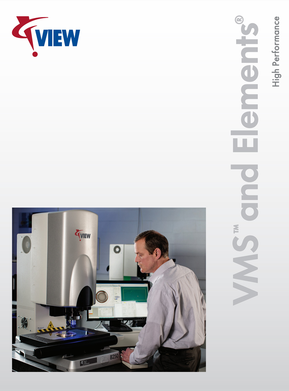
VMS® and Elements® Software
In order for you to view this file we ask that provide us with some information.
[dlm_gf_form download_id="2109" gf_ajax="true"]
Thank you for your interest in
VIEW Full Product Line
In order for you to view this file we ask that provide us with some information.
[dlm_gf_form download_id="2110" gf_ajax="true"]
Thank you for your interest in
Bump on Die
In order for you to view this file we ask that provide us with some information.
[dlm_gf_form download_id="2117" gf_ajax="true"]
Thank you for your interest in
Bump on Die
In order for you to view this file we ask that provide us with some information.
[dlm_gf_form download_id="2042" gf_ajax="true"]
This website uses cookies to ensure you get the best experience on our website. By continuing to use this site, you agree to our use of cookies. Learn more.