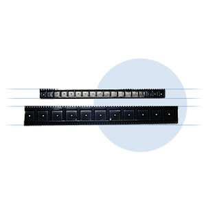
Non-contact measurement on chip carriers requires advanced lighting techniques and image processing capabilities in order to inspect and confirm critical pocket dimensions, such as hole location and size, as well as overall pocket length, width, and depth.
The high-volume nature of chip carrier production demands fast inspection cycles and sustained high throughput rates. Larger stage sizes and multiple light sources, such as backlighting and Programmable Ring Light (PRL), along with automated edge detection can be key factors for achieving required accuracy and throughput levels.


