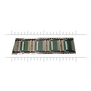
Flip chip processes present a number of critical metrology challenges including the need for precise three-dimensional measurements to accurately inspect pad size, position, and distance from the package edges as well as confirming acceptable flatness and coplanarity.
Accurate and efficient non-contact inspection of flip chips often requires advanced features such as multiple levels of magnification, Programmable Ring Light (PRL), and integrated lasers to improve inspection throughput rates.
In order for you to view this file we ask that provide us with some information.
[dlm_gf_form download_id="2111" gf_ajax="true"]
Thank you for your interest in
Flip Chip
In order for you to view this file we ask that provide us with some information.
[dlm_gf_form download_id="2115" gf_ajax="true"]
Thank you for your interest in
Flip Chip
In order for you to view this file we ask that provide us with some information.
[dlm_gf_form download_id="2114" gf_ajax="true"]
Thank you for your interest in
Flip Chip
In order for you to view this file we ask that provide us with some information.
[dlm_gf_form download_id="2113" gf_ajax="true"]
Thank you for your interest in
Flip Chip
In order for you to view this file we ask that provide us with some information.
[dlm_gf_form download_id="2116" gf_ajax="true"]
Thank you for your interest in
Flip Chip
In order for you to view this file we ask that provide us with some information.
[dlm_gf_form download_id="2118" gf_ajax="true"]
Thank you for your interest in
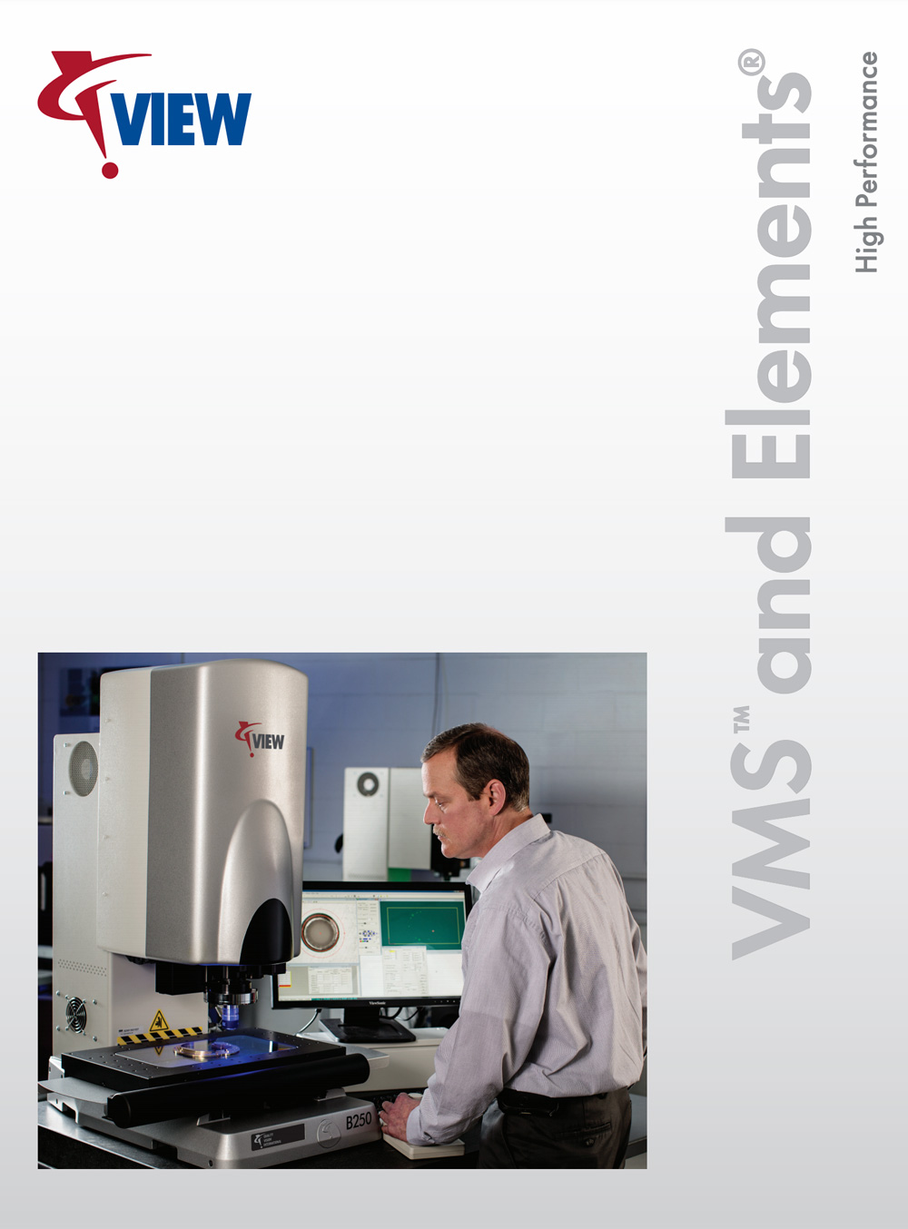
VMS® and Elements® Software
In order for you to view this file we ask that provide us with some information.
[dlm_gf_form download_id="2109" gf_ajax="true"]
Thank you for your interest in
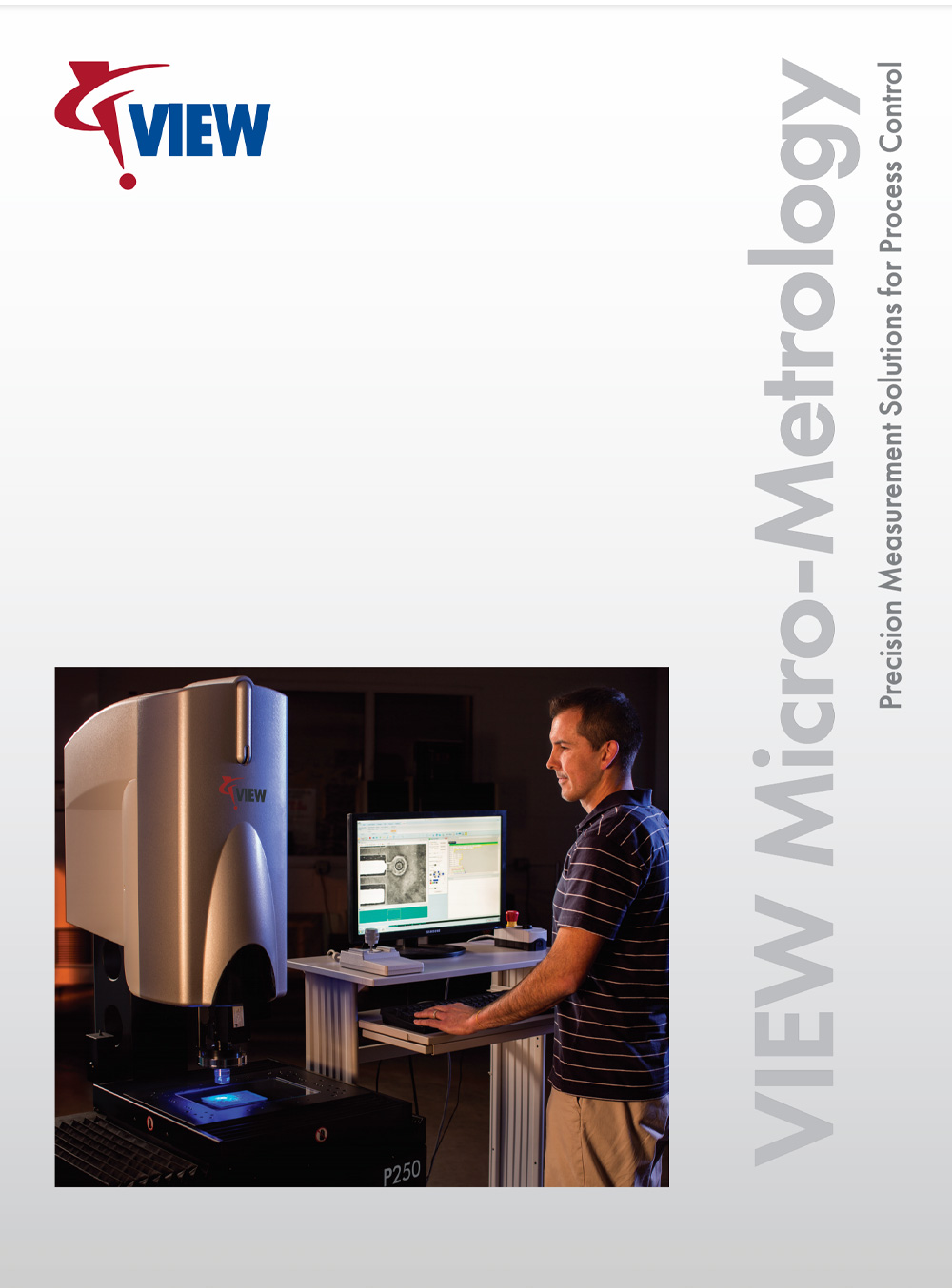
VIEW Full Product Line
In order for you to view this file we ask that provide us with some information.
[dlm_gf_form download_id="2110" gf_ajax="true"]
Thank you for your interest in
Flip Chip
In order for you to view this file we ask that provide us with some information.
[dlm_gf_form download_id="2117" gf_ajax="true"]
Thank you for your interest in
Flip Chip
In order for you to view this file we ask that provide us with some information.
[dlm_gf_form download_id="2042" gf_ajax="true"]
This website uses cookies to ensure you get the best experience on our website. By continuing to use this site, you agree to our use of cookies. Learn more.